Research
1. Optical study of semiconductors, electronic materials, and their nano-structures by using spectroscopic ellipsometry
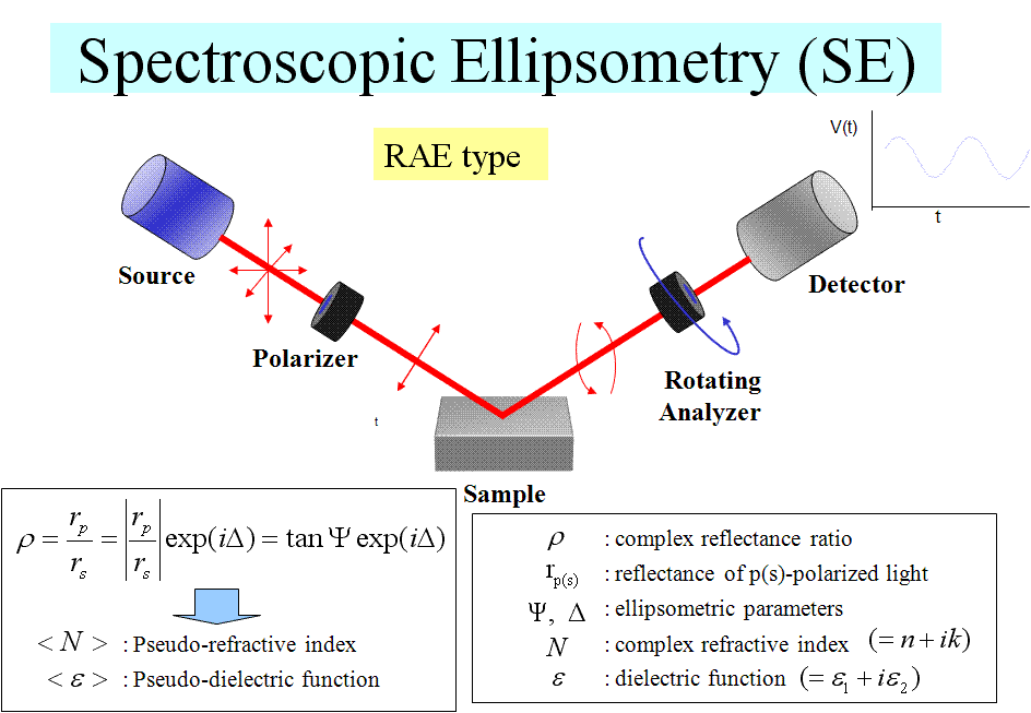
Spectroscopic
ellipsometry is a versatile and powerfull optical spectroscopy which estimates
the dielectric functions
and the thicknesses of multilayers. It measures
the ellipsometric angles ( Psi, Delta) which are related to the ratio of the reflectivity
of p- and s-polarization. Using multi-layer modeling analysis on the ellipsometric
angles, we can estimate the complex dielectric functions
which are
the square of the complex refractive indexes. From the dielectric functions,
we can determine the critical points
which are the symmetry points in the
electronic band structure where the conduction band and the valence band is
parallel.
2. Real-time spectroscopic ellipsometry including temperature dependence and in situ etching etc.
Real time spectroscopic ellipsometry usually uses white light source and
a very fast detection system such
as charge coupled detector (CCD) because
we measure the samples which are under growth or under rapid etching.
They
are usually attached to a vacuum chamber or plasma etching chamber. Therefore,
we can study a crystal growth mode
or surface morphology (states) during
etching.
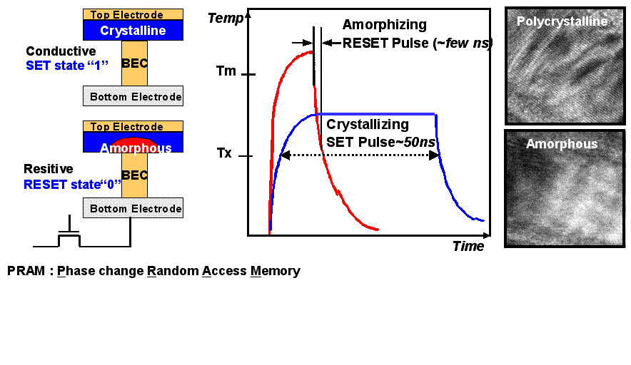
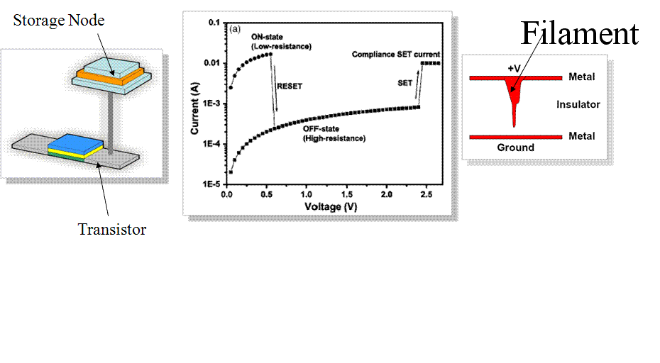
3. Materials and Devices of non-volatile memories- PRAM and RRAM
Non-volatile random access memory (NVRAM) device
does not lose memory even when the applied voltage is turned-off.
Presentl,
flash memory made of silicon is widely used. However, it has a slow speed
and a limit to device size. In order to circumvent
the disadvantages, other
NVRAMs are intensively investigated in the leading world laboratories. PRAM
(Phase change RAM) utilizes
high resistance (amorphous) and low resistance
state (crystalline phase) of chalcogenides materials such as Ge2Sb2Te5,
where
phase change is induced by Joule heat. RRAM (resistance switching RAM) devices
uses the resistance switching of oxides materials
induced by a sort of filmentation
induced by the applied electric field. The resistance switching does not involve
phase change,
but creation of current path in the medium. The mechanism
of RRAM is not established and is believed due to both
the mobile oxygen
ions and inetrface properties with electrodes. Using ellipsometry and I-V measurement
systems, we can investigae
the physical properties of the NVRAMs.
4. Electronic band structure of organic semiconductors e.g. functionalized DNA thin films
Bio-molecules and polymers are of increasing
interest in particular in the field of nanotechnology and the development of
new functional materials.
Deoxyribonucleic
acid (DNA) is a nucleic acid that contains the genetic instructions.
Chemically, double strand DNA(dsDNA) consists of
two long polymer chains of
simple units called nucleotides, with backbones made of sugars and phosphate
groups joined by ester bonds.
These two strands run in opposite directions to
each other and are therefore anti-parallel. Attached to each sugar is one of four
types of
molecules
called bases. In addition to its size in the nanometer
scale range, the DNA assembles spontaneously. It is believed therefore
to be a
promising candidate for designing new nanostructured materials. The possibility
to use the dsDNA as a programmable material
for nanotechnology applications has
sparked intensive research in the field. Structural modifications of water-soluble natural
DNA
and synthesis of organic-soluble DNA are of high technological interest in
diverse fields such as development of bio-sensors
or new types of electronic
and optoelectronic devices. A central issue for designing such organic
hybrid devices is the determination of structural,
electronic and optical
properties of organic films. By using ellipsometry and Raman spectroscopy, we
investigated the electronic propeerties
of functionalized DNAs.
LED made with CTMA DNA as hole transport layer.
![]()